Tool Owner - Dr. Michael Shafer
START USING THIS TOOL
- Step 1: ONLINE
- Step 2: HANDS - ON
- Step 3: ACCESS
Quick Links:
Keyence VHX-7000
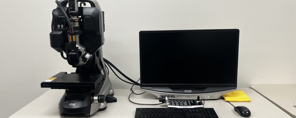
Instrument Overview
The Keyence VHX-7000 is our flagship optical metrology system, bridging the gap between traditional optical microscopy and SEM (Scanning Electron Microscopy). It utilizes a 4K CMOS sensor and advanced lighting algorithms to capture fully-focused images of uneven surfaces instantly.
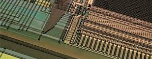
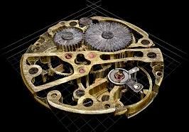
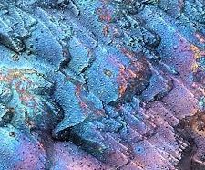
SAMPLE GALLERY
Features
Capture ultra-detailed images across a wide magnification range—ideal for quickly spotting micro-defects, edge wear, and fine surface features without losing clarity.
Automatically combines multiple focus layers into one fully in-focus image, so uneven or tall samples stay sharp from top to bottom.
Builds a 3D surface map to visualize and quantify height variations—useful for steps, pits, scratches, and general topography checks.
Fast, repeatable measurements (distance, angle, area, diameter, etc.) with minimal manual input—great for consistent inspection and reporting.
TECHNICAL SPECIFICATIONS
- Sensor – 1/1.8-inch CMOS image sensor
- Effective Pixels – 3840 (H) x 2160 (V)
- Frame Rate – 50 fps (max)
- Illumination – High-intensity LED (Ring, Coaxial, Mixed)
- Stage – Motorized XYZ with 100mm x 100mm travel
- Data Output – .JPEG, .TIFF, .CSV (Measurement data)